Which Via Should I Choose? A Guide to Vias in PCB Design
When Should I Use Vias?
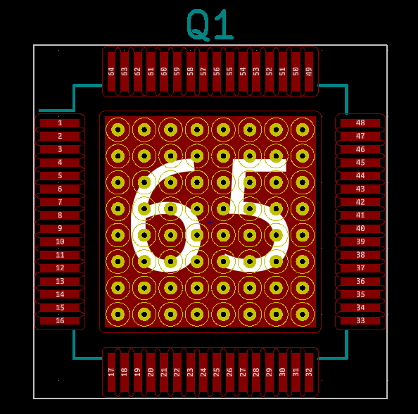
Vias provide a path for electrical and thermal energy to move from layer to layer on your board. Generally, the more energy being dissipated by an IC, the more vias it should have connecting its thermal pad to the underlying copper layers that can distribute the thermal energy.

A thermal pad for the QFN IC has 64 vias!
For parts of your circuit carrying power, or fast signals, use multiple vias to connect layer to layer. It is generally better to have several smaller vias than one large via. The design choice reduces inductance and provides additional paths for current in case one of the vias fails.
Types of Via
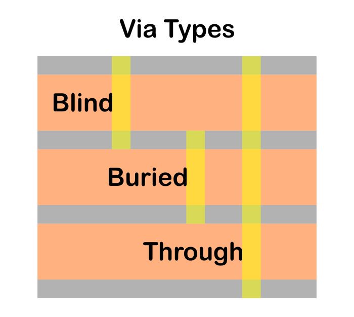
There are three basic kinds of vias:
- Blind vias: connect an exterior layer to an interior layer
- Buried vias: connect two interior layers
- Through vias: connect two exterior layers

For a simple two-layer board, your only option is a through via. For boards with more than two layers, you might also be able to specify blind or buried vias in your design (at increased cost).
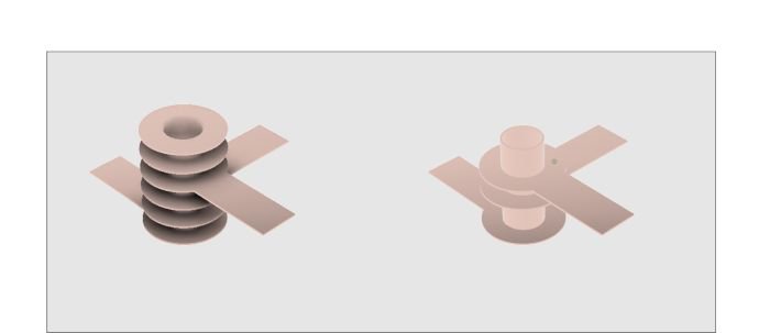
It is often the case that a via needs to form an electrical connection between internal and external layers. The use of a through-hole via in such situations places an unused hole (and possibly an unused pad) onto other layers, and this consumes PCB real estate and interferes with routing on adjacent layers, but it is the cheapest and most reliable option. Blind vias can free up real estate by creating a connection between the two layers and a hole only on the layers in between. Buried vias are not often used due to expense, reliability concerns, and difficulty of troubleshooting.

What Kind Should I Use?
Through vias are generally the least expensive via type to include on your design. Blind and buried vias should be discussed with your manufacturer prior to board layout to determine their capabilities.
How Do I Use Blind and Buried Vias in My Design?
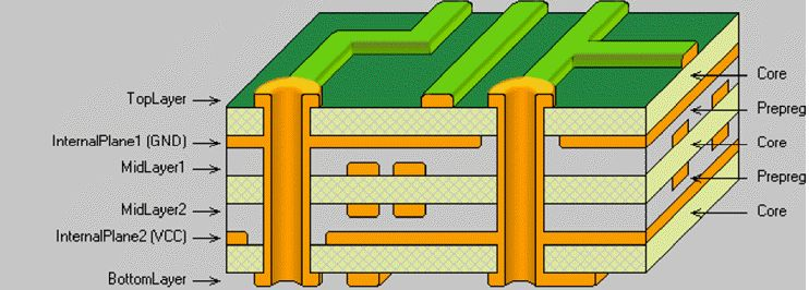
It’s important to remember that when PCBs are manufactured, each layer consists of two sheets of copper separated by a dielectric core.

Image shows a PCB stackup with through vias and assorted copper traces.
These layers can be assembled in a variety of fashions during manufacture, allowing a combination of blind buried vias. Your computer software likely will allow you to specify which layers you would like to connect, but it most will not stop you from making choices that cannot be manufactured. If you cannot recreate your stackup with cardboard and a stapler, without bending or tearing the cardboard, your PCB manufacturer cannot make your board.
What Size Should Vias Be?
Check with your manufacturer for their minimum drill size and minimum annular ring for the manufacturing process they will use. Typical mechanical drills don’t go much lower than 12 mil in diameter without frequent breakage, so the manufacturer will increase the cost to account for broken drills. Annular rings don’t often go below 6 mil for standard processing. So the smallest via you would create has a 12-mil diameter hole, and a 24-mil diameter pad.
Please login and click here to download the PDF file:


