

How large is Gold Phoenix?
What is GP’s Privacy Policy?
What happens if I have a problem?
What is your company’s the lead time?
How do you keep your prices low?
How can I know Gold Phoenix is dependable?
How GP control the quality?
How to reduce the cost of printed circuit board?
Why there is a setup fee?
What kind files your company needed to make PCB?
What is V score Vs Tab-routing?
Do you charge extra fee for different color of solder mask such as blue, red, yellow, black?
When should I have my boards electrically tested?
Does GP bevel gold fingers?
What does CNC Rout points mean?
Are you MIL SPEC 55110 approved?
To what acceptability standards do you build?
Why do I need to allow for more space between copper features when ordering thicker copper?
What is Gold Fingers?
In 2011, Gold Phoenix has more than 300 employees in China, our sales volume is around 1Million dollars/month. We are one of the biggest customers of FEDEX and DHL.
2. What is Gold Phoenix’s Privacy Policy?
At Gold Phoenix we recognize that privacy is of utmost importance, and we do not sell or rent any individual personal information to any third party.
3.What happens if I have a problem?
We are committed to your satisfaction and we ask that you contact your salesperson immediately if you have a problem of any kind. You can file a complaint on our website; the case will be closed only when you are 100% happy. Also, we would like to hear any suggestions you may have for improvements. You can also check our warranty at http://www.goldphoenixpcb.com/html/qca/warranty/index.html.
4. What is your company’s the lead time?
For prototype orders 2 layers we can do 8 hours, 1 day return and 3 days return or 5-7 days return (standard time). 4-8 layers 6 days; 10-12 layers 12 days. Production orders around 10-12days
The price info is listed on
http://www.goldphoenixpcb.com/pcb-special-price.html
5. How do you keep your prices low?
We keep our prices low by constantly implementing more efficient manufacturing processes, developing systems that allow us to quickly change setups, maintaining partnerships with suppliers, and conservatively managing our business. Also the our factory is located in China, the labour cost is low in China.
6. How can I know Gold Phoenix is dependable?
You can use Google to search our company, we are very popular PCB house online. You can also check http://myworld.ebay.com/tigeryesh. We sell PCB boards on ebay for 3-4 years, our feedback is 100%!
1. How to reduce the cost of printed circuit board?
The PCB price is related with size, min clearance, min hole size, and number of layers. If you just get the lowest price please design your board as simple as possible. For the standard spec of the PCB will be : 2 layers 0.062”, FR4 , 1oz, HAL, hole size>15mil, clearance>7mil, square shape, without slots. You can also get more info from our document “PCB Cost Cost Analysis of Printed Circuit Board”
2. Why there is a setup fee?
Setup fee is charged for one-time only. It is the photo fee used for etching the PCB. At high quantity there is no setup fee. We just charge unit price per board.
3. What kind files your company needed to make PCB?
We need Gerber files 274X files, and NC drill files to make PCB.
Bottom copper layer ; Top copper layers; Inner layer1( for multi-layers); Inner layer2 (for multi-layers); silkscreen top; silkscreen bottom (if you have); top solder mask and bot solder mask; Border layer( Layer used to define the shape of the board).
4. What is V score Vs Tab-routing?
V scoring is probably faster and easier but has limitations. It an only work with square shape, and V score line can only go from edge to edge. Once assembled the scored grooves can be sliced apart using what is sometimes called a pizza cutter type de-paneler or even snapped apart depending on design and how close the component lands are to the edge of the boards.
Tab routing can handle odd shapes but usually leaves nubs or small pieces of laminate on the edges that may need to be sanded off. Also, tab routing in high volumes takes a lot of time on the router and may drive your cost up.
If the vendor has scoring in house and the boards are square that would probably be the cheapest but if they have to send out for scoring that can drive up cost. Some tabs also have small holes drilled into them to help the breaking apart of the individual boards but again, this can drive up cost. If you use tab routing make sure you make the tabs big enough to be strong and make an array that can be handled but not so big that the boards cannot be broken apart.
5. Do you charge extra fee for different color of solder mask such as blue, red, yellow, black?
For high quantity there is no extra charge. For small orders cost extra USD20, you can check http://www.goldphoenixpcb.com/pcb-special-price.html for more info.
6. When should I have my boards electrically tested?
GP give free testing for all boards more than 2 layers. We feel that Electrical Test is an essential component to the PCB 's manufacturing process, however in rare instances customers may determine that the added expense is not justified in particular situations. It is only to accommodate these situations that we break out this process as an option.
-Our goal is to ship all boards with zero defects and Electrical Test is a critical part of this quality process. While Electrical Test will not eliminate the possibility of any defects being present on boards that you receive it will significantly reduce the likelihood.
-When Electrical Test is ordered Gold Phoenix will warranty the bare boards for defects in materials and workmanship for 90 days from date of shipment. We will replace or issue credit for any bare boards that are returned and confirmed by GP to be non-conforming to the order specifications and/or the applicable quality and acceptability standards. We will not accept liability for any cost in addition to the value of the bare boards including but not limited to components, labor, business interruptions and any other consequential damages or losses.
7.Does GP bevel gold fingers?
Yes. We do bevel gold fingers unless otherwise specified. We do NOT bevel solder fingers unless specified by customer.
8.What does CNC Rout points mean?
Each corner or"turn" on your pcb is a rout point - that is every time the router bit turns or stops. Each radius is three points. Count 8 for a circle and for each tab-routed pcb in an array configuration. More than 6 routing points will be consider as complex shape board by GP.
9. Are you MIL SPEC 55110 approved?
No. However, you can Prototype (Standard Spec) with us because we use the same materials, specifications, and processes. GP is UL approved, our UL code is lised on the home page.
10.To what acceptability standards do you build?
IPC-A-6011/6012 latest revision with inspection based on IPC-A-600 latest revision: Class 2 Prototypes (Standard Spec) and Class 2 Production (Custom Spec). We can also make boards need comply with IPC Class 3.
11.Why do I need to allow for more space between copper features when ordering thicker copper?
Glad you asked!
The most common unit of measure for the copper thickness on a printed circuit board is ounces (oz). But how thick is that? It's the resulting thickness when 1 oz of copper is pressed flat and spread evenly over a one square foot area. This equals 1.37 mils (1.37 thousandths of an inch).
Most PCBs are constructed with 1 oz copper thickness. At Gold Phoenix, if we are not given specific specs, we will assume 1 oz when quoting and building your design. If you have determined that your design requires more current than 1 oz can carry, you'll need to consider increasing the copper weight or increasing the width of your traces.
Of course the thicker the copper the higher the cost, but there are certainly times WHERE this is necessary. The cost increase is not only due to the raw material costs but processing thicker copper weights takes more time and is a little trickier to do. Etching the spaces (air gap) between traces is more difficult than etching a trace of the same width as your space.
Bare Laminate
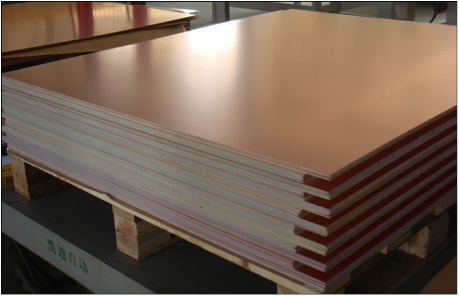
Printed circuit board material is purchased from the laminate supplier pre-clad with copper on both sides. The laminate looks like a solid sheet of copper. This pre-clad material comes in various laminate and copper thicknesses so PCBs can be constructed with different thicknesses and finished copper weights.
Imaging
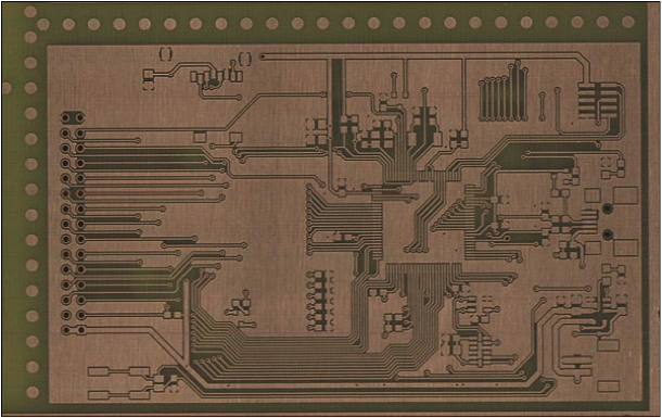
Because the production panels are completely covered with copper, the excess copper needs to be removed to reveal your design. To do this, a 1:1 size image of your design is photo plotted onto a film. The copper clad panel is coated with an etch-resistant material and your image is then transferred onto the etch resist.
Etching
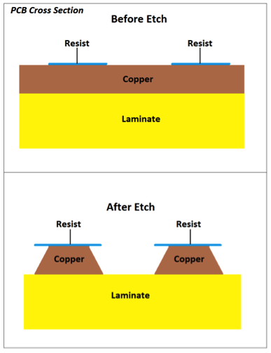
Next, the panel is submerged in a chemical bath where only the protected areas of the panel will have copper remaining. This is where the spacing between your copper features are critical.
Etching is a subtractive process, meaning excess material is removed; therefore, there is no way to prevent the chemical solution from removing the sides of the traces as it etches down toward the bare laminate.
As soon as the chemicals begin etching down toward the laminate, they also begin etching laterally underneath the resist. Since the copper closest to the resist will be exposed longest, these areas will have the most lateral etching resulting in a trapezoidal shape to copper features. As you can imagine, the thicker the copper, the more time it will take for the solution to etch all the way down to the bare laminate to define your pattern.
One of the many things that is done during the tooling and setup of your order is the size of your copper features are slightly increased to compensate for lateral etching. This compensation will reduce the spacing between features. This, combined with the longer required time spent in the etchant, is why more space is needed between elements on thicker copper boards. If elements are too close together, it won't be possible to etch down to the laminate before the copper features are reduced too significantly or are etched completely away.
Gold fingers are the gold-plated connectors that are on the edges of the printed circuit board. They are similar to fingers in that they are long and narrow.
Why Do Gold Fingers
Gold contact surfaces are often used on circuit boards with membrane switches which are a technology of choice for industrial, commercial and consumer products. When PCBs will be repeatedly installed and removed electroplated gold is used for edge-connector contacts or as they are more commonly known: Gold fingers. It is a card-edge connector when need insert this board to other devices such as motherboards, chassis, etc. also be called bonding finger as it need plate gold on Copper nickel layer.
Gold and Thickness
The connectors where circuit boards connect to other boards are usually gold plated. Gold is ideal for any connection application because it is an excellent conductor, is easily plated and is extremely resistant to tarnish.
Usually, fingers are done by hard gold or immersion gold. The gold thickness is requested to be from 5 micro inches to 15 micro inches. 30 micro inches to 50 micro inches are also chose by many customers because fingers are mainly used for plugging many times.
Holes in Fingers
It is up to you to define the length of gold fingers and relate this info to the fabricator. We do not suggest putting holes in fingers area. If you have holes in the fingers area, it's better non-plated holes.
Bevel and Chamfer
Normally in order to insert the PCB board to other devices slot smoothly, gold fingers need bevel.
The gold finger bevel default value: 45 angles.
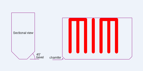
Chamfer Angle range: 20°?¢30°?¢45°
Chamfer depth: L
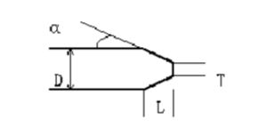
Formula for Chamfer depth: L=(D/2-T/2)/tgα
D£oboard thickness (mm) T£osurplus thickness (mm)
α£oChamfer Angle L£oChamfer depth (mm)
A few design rules are required for gold fingers /edge connectors:
1, No solder mask or silk screening can be present in the plated area
2, For panelization, always place gold fingers facing outward from the panel center
3, We do bevel gold fingers unless otherwise specified. We do NOT bevel solder fingers unless specified by customer.
Section
FAQ_1
Tel:1-888-PCB-9518 or 1-888-722-9518
Email:sales@goldphoenixpcb.biz,
goldphoenixtech@yahoo.ca
Copyright Gold Phoenix PCB Co., Ltd. 2011 - 2016

