

How to Create a Printed Circuit Board (PCB)(Section 2)
2. Prototyping
With a basic idea in mind, a circuit schematic is developed and analyzed to ensure the desired functionality and performance. When creating a circuit for PCB production, a designer would also select specific components at this time. Commonly, the next step is to prototype and to test the circuit. It is also possible to use the schematic capture software along with related software to simulate the circuit without building it on a prototyping board.
In the case of the example optosensor circuit (see Fig. 2), a rough sketched schematic was initially created, along with some design specifications. The necessary components were chosen and the circuit was built on a prototyping board to verify that it met the design criteria. During the prototype board layout phase, thought was given to the best way to arrange the components for the final PCB layout. As a result, the PCB layout is very similar to the protoboard layout you see in Fig 2.
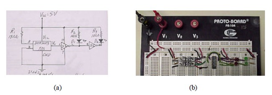
Fig 2: The optosensor circuit: (a) hand-drawn schematic and (b) prototyped circuit.
Gold Phoenix PCB Quality Control
Product Quality: DRC Check, Electrical Testing, AOI(Automated Optical Inspection), ISO9001:2008, UL:E306317 and RoHS
PCB Assembly Quality Control System: X-Ray Inspection for BGA Assembly, Components Quality control, Assembly Quality Control and Ultrasonic PCB Cleaning
https://www.goldphoenixpcb.com/html/qca/pqcs/index.html
Section
1. Overview
2. Prototyping
6. Lessons Learned and Recommendations
7. Appendix