How to Create a Printed Circuit Board (PCB)(Section 1)
1.Overview
There are several basic steps involved in producing a printed circuit board (PCB). Most designs begin with a hand drawn schematic and design plan. With these, the circuit is prototyped and tested to verify that the design works correctly. Then, using software, an electronic version of the schematic is created. A netlist file is created from the electronic schematic and used in other software to create the physical layout of the PCB. Next, the components are placed and routed in the physical layout software and Gerber files are created. These Gerber files are used in a prototyping system to mill, drill, and cut the PCB substrate. The components are then placed and soldered to the substrate. Finally, the board is tested to verify that it works as expected.
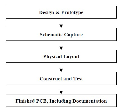
The major steps in the PCB design and fabrication process are as follows:
1. design and test the prototype circuit—by hand;
2. capture the circuit's schematic—using OrCADCapture or similar software;
3. perform the physical layout of the circuit—using OrCADLayout or similar software;
4. fabricate, populate and test the PCB—done by ECE shop personnel or similar personnel.
With this general procedural framework in mind, read on to learn more about each step in this process (see Fig. 1).

Fig 1: PCB design flow.
Safe & Easy Shopping at Gold Phoenix PCB
90 Days Limited Warranty
OEM Import Tax Exemption
ISO9001:2008
UL:E306317
DigiCert SSL Certificate
Mastercard/ Paypal/VISA
https://www.goldphoenixpcb.com/
Section
2. Prototyping
6. Lessons Learned and Recommendations
7. Appendix


