RF Layout & wiring
1、RF Layout
The discussion here is mainly about the placement of components in the laminates. The key to component location layout is to fix the device on the RF path. By adjusting its direction, the length of the RF path should be minimized, and the input should be far away from the output. High power circuit and low power circuit should be separated as far as possible, and sensitive analog signals should be far away from high speed digital signals and RF signals
The following techniques are often used in layout.
1.1 Line-shape layout
The components of the RF main signal should be arranged in line shape as far as possible, as shown in Figure 1. However, due to the limitation of PCB board and cavity space, it can't be arranged in a line shape in most cases. At this time, L shape can be adopted, and U shape layout is best avoided (as shown in Figure 2). Sometimes, if it is unavoidable, try to widen the distance between input and output as far as possible, at least 1.5cm above.

Figure 1 Line-shape layout
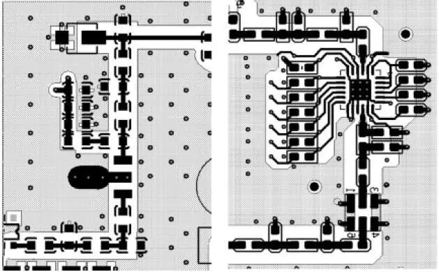
Figure 2 L-shape and U-shape layout
In addition, when using L-shape or U-shape layout, it is better not to turn at the turning point just after entering the interface, as shown in Figure 3 on the left, but to turn after a little segment of the line, as shown in figure 3 on the right.
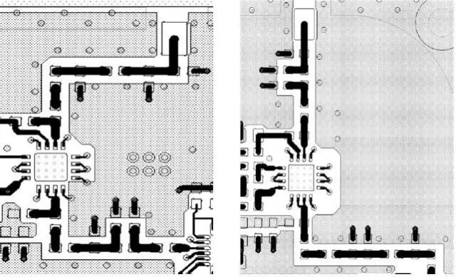
Figure 3 2 plans
1.2 Same or symmetrical layout
As far as possible, the same modules have the same or symmetrical layout, as shown in Figure 4 and Figure 5
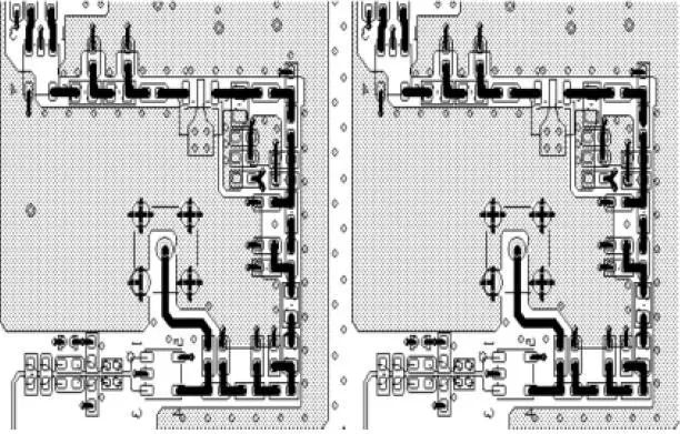
Figure 4 same layout
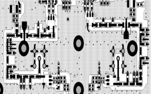
Figure 5 symmetrical layout
1.3 Cross layout
The bias circuit's feed inductance is placed vertically with the RF channel, as shown in Figure 6, mainly to avoid mutual inductance between inductive devices
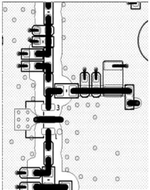
Figure 6 cross layout
1.4 45° layout
To make rational use of space, the components can be arranged in a 45-degree direction to keep the RF line as short as possible, as shown in Figure 7.
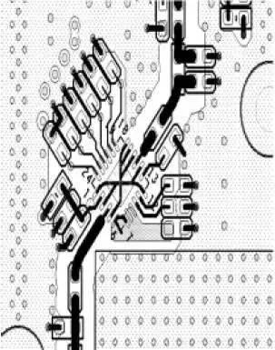
Figure 7 45° layout
2、RF wiring
The overall requirements of wiring are: RF signal line is short and straight, reduce line mutation, less holes, do not intersect with other signal lines, RF signal line around as much as possible through the hole
Here are some common optimizations:
2.1 Gradient line processing
When the RF line width is much larger than the pin width of IC device, the line width of the contact chip adopts a gradual approach, as shown in Figure 8.

Figure 8 gradient line
2.2 Arc-line processing
When the RF line is not straight, the circular arc processing can reduce the RF signal's external radiation and mutual coupling. It has been proved by experiment that the Angle of transmission line can reduce the return loss to the greatest extent. See Figure 9
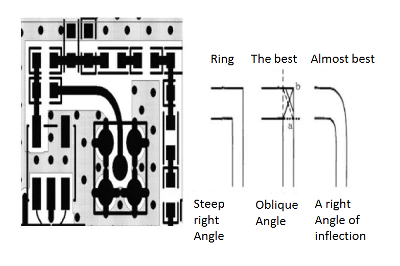
Figure 9 Arc line
2.3 Ground wire and power supply
The ground wire is as thick as possible. Under the condition of conditions, every layer of PCB should be laid as far as possible, and the ground should be connected to the main ground, and more holes should be punched to reduce the ground impedance as far as possible.
RF circuit power should not use plane segmentation as far as possible, the whole block of power supply plane not only increases the radiation of the power supply plane to RF signal, but also easy to be interfered by RF signal. Therefore, the power line or plane generally adopts the shape of a long strip, which is processed according to the size of the current. It is as thick as possible under the premise of meeting the current capacity, but it cannot be widened unlimitedly. When dealing with power lines, be sure to avoid forming loops.
The direction of the power line and ground should be parallel to the direction of the RF signal, but should not overlap. WHERE there is a cross, it is better to use the way of vertical cross
2.4 Cross processing
The RF and IF signals cross each other and try to keep a space between them.
When RF signals cross with other signals, try to arrange a layer of ground connecting with the main ground along the RF line between them. If that's not possible, make sure they're crossed. Other signals in this case also include the power line
2.5 Ground processing
The ground processing of RF signal, interference source, sensitive signal and other important signals can not only improve the anti-interference ability of the signal, but also reduce the interference of the signal to other signals. See Figure 10
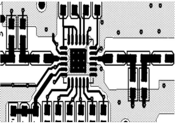
Figure 10 Packet processing
2.6 Copper foil processing
Copper foils shall be smooth. Long lines or sharp corners are not allowed. Otherwise several holes shall be filled at the edges of sharp corners, slender copper foils or copper foils
2.7 Spacing processing
The RF line shall be at least 3W wide from the edge of the adjacent ground plane, and there shall be no ungrounded through-holes within the 3W range

Figure 11 Space
The RF lines in the same layer should be grounded and perforated in the copper skin. The spacing of the holes should be less than 1/20 of the wavelength of signal frequency (λ), and they should be evenly arranged. The width of the edge of clad copper skin from the radio frequency line 2W or the height of 3H, where H represents the total thickness of the adjacent medium layer.
Capabilities
Payment Methods
Specials Price
Carriers
Support Hobbyist
Certificate
Customer Support
Follow Us
Tel: 1-905-339-2881
Email: sales@goldphoenixpcb.com , tech@goldphoenixpcb.com
Copyright Gold Phoenix PCB Co., Ltd. 2011 - 2026
Tel: 1-905-339-2881 Email: sales@goldphoenixpcb.com , tech@goldphoenixpcb.com
Quality Control System
|
Products/Service
|
Friendly Links
Copyright Gold Phoenix PCB Co., Ltd. 2011 - 2026


