Knowledge Center
This Gold Phoenix PCB Knowledge Center article explains electromagnetic interference (EMI) shielding for flexible circuits, covering copper layers, silver ink, shielding films, and reliability considerations.
The integrity of electronic circuits is important to the reliable operation of devices used daily. One pervasive challenge can disrupt this reliability: Electromagnetic Interference.
EMI is not just a technical nuisance; it can degrade the performance of electrical circuits, elevating error rates, generating significant noise within signals, or in severe cases, causing total data loss. Imagine the chaos if the electronics in medical devices, smartphones, or aerospace navigation systems faltered due to EMI!
Understanding EMI is the first step in mitigating its effects. EMI is a disturbance generated by an electrical source affecting another circuit through electromagnetic induction, electrostatic coupling, or conduction. The repercussions? Compromised device functionality or complete failure. However, this challenge is one that has been studied and examined over many years within the industry, identifying shielding as a straightforward solution that can be incorporated into many designs. In this case, the answer is shielding — a defense mechanism implemented at the circuit level.
Shielding at the circuit level is both a strategy and a cost-effective precaution. By applying shielding close to sensitive circuits, the overall cost of protection can be reduced. But how is this shield implemented? Three methodologies stand out for EMI protection.
Copper layers are a common and generally straightforward solution for EMI shielding. By adding extra copper layers around the critical signals, a protective encapsulation is created, mirroring strategies used in rigid PCB designs. These copper shields, preferably solid for maximum protection, are interconnected to the ground circuit via a row of via holes flanking either side, crafting a near-impenetrable cage against EMI. Yet, flexibility is a consideration; thus, cross-hatching is employed, when necessary, though while recognizing the potential compromise in shielding effectiveness and using it in limited amounts.
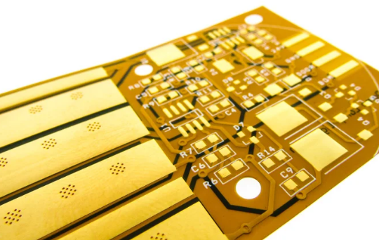
Flexible circuit board manufactured with copper shields.
Silver ink shielding uses a printed conductive layer. This method involves screening a layer of silver epoxy ink onto the external surfaces of the primary coverlay, then encapsulating it with a secondary coverlay. The silver ink forms a conductive pathway to the ground through the coverlay openings and vias, ensuring the shield is connected to ground.
While this method adds complexity, time, and cost due to additional processing steps and materials, its established use in EMI shielding reflects its effectiveness and reliability. Unfortunately, to this day, silver ink has been slowly phased out in favor of copper layers and shielding films due to its limitations for high density component areas and a driving need for thinner flex circuits.
Developed in response to the need to protect delicate electronics from EMI, shielding films have become an important option for flexible circuit protection. Comprising an electrically conductive adhesive, a metallic deposition layer for shielding, and an outer insulating flexible epoxy, these films provide a shielding solution while maintaining a thin profile and cost-effectiveness.
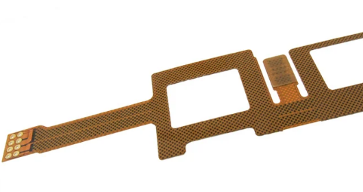
Flexible circuit board manufactured with shielding films.
They connect to the ground in a similar fashion to silver ink but require no secondary coverlay, thanks to their built-in insulation layer. This not only simplifies the application process but also enhances their capabilities, making them suitable for a wide array of applications, including rigid-flex circuits. However, this film is not a perfect solution; for example, stiffener adhesion may require alternative solutions such as pressure sensitive adhesives rather than typical stiffener lamination procedures.
The process does not end with selecting the shielding methodology. Ensuring that the final product can withstand the rigors of its application, especially in flexible designs, is crucial. For instance, in flex circuits, the incorporation of via holes to stitch shielding layers together requires a careful balance to maintain flexibility and prevent stress concentrators that could lead to cracks. Adherence to design standards, such as IPC 2223 for flex and rigid-flex, and thorough bend requirement reviews are vital steps in this process.
As electronic applications become more widespread, the need to address EMI will continue to grow. The methodologies discussed — copper layers, silver ink, and shielding films — represent available approaches for addressing EMI. Each brings its unique strengths to the table, from the robustness of copper layers to the flexibility of shielding films.
By integrating these solutions into circuit designs, these methods not only protect against EMI but also ensure the reliability and longevity of electronic devices that have become indispensable in daily life. These shielding solutions help preserve circuit performance and reliability against problems that can arise from electromagnetic interference.
Capabilities
Payment Methods


Specials Price
Carriers


Support Hobbyist
Certificate


Customer Support
Follow Us