

Printed Circuit Design Tutorial (Define the design rules for the PCB)
B.Define the design rules for the PCB
After define the PCB shape the next step is to define the design rules. Most of the PCB software can define those design rules before the PCB layout, then you can make sure the PCB is designed in the right specification.
1)Min clearance& Min hole size
Min clearance means space between different networks. Usually if you want design a low cost PCB setup the clearance 7mil-10mil, and we suggest>=10mil. One example is shown in Fig 3.
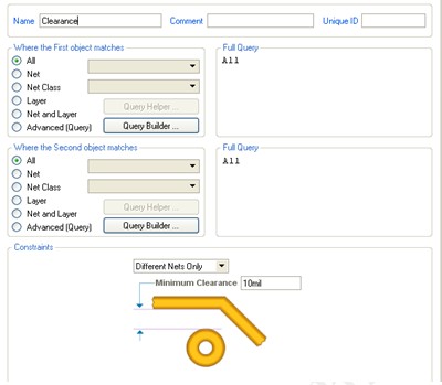
Fig 3 Define the Minimum clearance
When you use the via make sure the min hole size is>10mil, for a low cost PCB the via diameter>15mil and the pad around the via diameter >23mil, which will give a min ring of 8mil. One example is shown in Fig 4. If space is not a problem always try to have a min 15mil hole and 10mil ring.
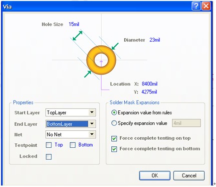
Fig 4 Define the via and ring
There is only min size limitation, so it is not a problem to define a larger clearance or hole size. The definition hole size is the "finished" hole size in the PCB and has a +/-3-5mil tolerance. Trace width on the final PCB will has tolerance +/-15%-20%.
You can also define other design rules some rules are shown in Fig 5, and those rules will not be explained one by one. Most of time we only need to define the electrical rules and use default setting for other rules.
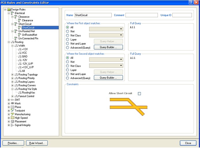
Fig 5 Other rules for the PCB design
Printed Circuit Design Tutorial
Section
1. Basic rules in PCB Design : The size and shape of the PCB
2. Basic rules in PCB Design : Define the design rules for the PCB
3. Printed Circuit Design Tutorial (A. V Score)
4. Printed Circuit Design Tutorial (B. Tab-routing)
5. Printed Circuit Design Tutorial (C. Define Non-plated holes - NPTH)
6. Printed Circuit Design Tutorial (D. PCB finishing)
7. Printed Circuit Design Tutorial (E. Solder mask)
8. Printed Circuit Design Tutorial (F. Silk Screen)
9. Printed Circuit Design Tutorial (G. Copper thickness and Via current handling capacity)
10. Printed Circuit Design Tutorial (H. Via)
11. Printed Circuit Design Tutorial (I. Slot)
12. Printed Circuit Design Tutorial (J. Voltage break points)
13. Printed Circuit Design Tutorial (K. Half hole design)
14. PREPARE MANUFACTURE FILES FOR PCB HOUSE
Please login and click here to download the PDF file: Download