Printed Circuit Design Tutorial (K. Half hole design)
K. Half hole design
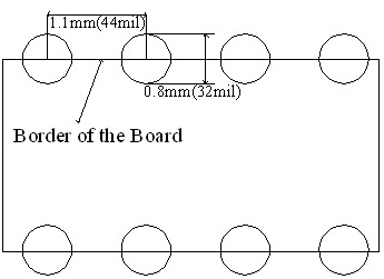
Half PTH holes are usually designed at the edge of the board, the holes are plated. The way to design this is just to put the holes at the edge of the board, and put the border line across the middleof the holes. The min hole size will need to be 0.8mm (32mil), the min clearance between the holes need to be 1.1mm from the center from one hole to another. There is no requirements for thesize of the pads, you can design the pads the same size as the hole.

Fig 18 Half Hole Design Example
Printed Circuit Design Tutorial
Section
1. Basic rules in PCB Design : The size and shape of the PCB
2. Basic rules in PCB Design : Define the design rules for the PCB
3. Printed Circuit Design Tutorial (A. V Score)
4. Printed Circuit Design Tutorial (B. Tab-routing)
5. Printed Circuit Design Tutorial (C. Define Non-plated holes - NPTH)
6. Printed Circuit Design Tutorial (D. PCB finishing)
7. Printed Circuit Design Tutorial (E. Solder mask)
8. Printed Circuit Design Tutorial (F. Silk Screen)
9. Printed Circuit Design Tutorial (G. Copper thickness and Via current handling capacity)
10. Printed Circuit Design Tutorial (H. Via)
11. Printed Circuit Design Tutorial (I. Slot)
12. Printed Circuit Design Tutorial (J. Voltage break points)
13. Printed Circuit Design Tutorial (K. Half hole design)
14. PREPARE MANUFACTURE FILES FOR PCB HOUSE
Please login and click here to download the PDF file: Download


