

Printed Circuit Design Tutorial (J. Voltage break points)
J. Voltage break points
There is an Experiments performed by UL in the course of analysis of silver PCB surface finish, demonstrated that the withstand voltage of a pair of parallel conductors is purely a function of conductor spacing, not surface finish. Based on the experiments, UL specified withstand voltage of 40 volts/mil or about 1.6 kW/mm in their test methods of UL796 Standard for Printed Wiring Boards. For exampl e, for working voltage 500V you need to meet the withstanding test voltage 1740 Vrms per UL 60950-1 Table 5B. Such AC signal has 1740* √2 =2461 V peak value. With the 40V/mils criterion, the required minimum spacing would be 2461/40=62 mils (or 1.6 mm). More info can be found at https://www.smps.us/pcbtracespacing.html
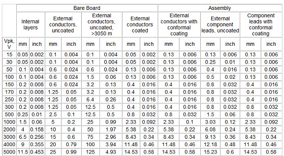
Fig 17 Clearance requirement of voltage level
Printed Circuit Design Tutorial
Section
1. Basic rules in PCB Design : The size and shape of the PCB
2. Basic rules in PCB Design : Define the design rules for the PCB
3. Printed Circuit Design Tutorial (A. V Score)
4. Printed Circuit Design Tutorial (B. Tab-routing)
5. Printed Circuit Design Tutorial (C. Define Non-plated holes - NPTH)
6. Printed Circuit Design Tutorial (D. PCB finishing)
7. Printed Circuit Design Tutorial (E. Solder mask)
8. Printed Circuit Design Tutorial (F. Silk Screen)
9. Printed Circuit Design Tutorial (G. Copper thickness and Via current handling capacity)
10. Printed Circuit Design Tutorial (H. Via)
11. Printed Circuit Design Tutorial (I. Slot)
12. Printed Circuit Design Tutorial (J. Voltage break points)
13. Printed Circuit Design Tutorial (K. Half hole design)
14. PREPARE MANUFACTURE FILES FOR PCB HOUSE
Please login and click here to download the PDF file: Download