

Printed Circuit Design Tutorial (G. Copper thickness and Via current handling capacity)
G. Copper thickness and Via current handling capacity
In PCB industry the thickness of the copper on the PCB is defined use oz. 1oz=35um. Thicker copper means the trace and pass more current.
This PCB track width calculator determines approximations to the ANSI/IPC-D-275 and IPC-2221 design standards for PCB trace / track width.

where:
W = Minimum required track width in mils
I = Maximum current in Amps
dT = Maximum allowable temperature rise above ambient in C
h = Thickness of the copper cladding in oz/ft^2
k = 0.024 for inner layers and k= 0.048 for outer layers
This calculator is accurate up to 35A current, up to 400mils of trace width, from 10C to 100C temperature rise, and copper of 0.5oz/ft to 3oz/ft. Outside of this ranges, calculator won't produce accurate results. The DC resistance of the trace can be calculated as below: for copper at 25 degree p=1.724X10⁻⁸ohm/meter, at 100 degree p=2.3X10⁻⁸ohm/meter. AC resistance is more complex due to skin effect.
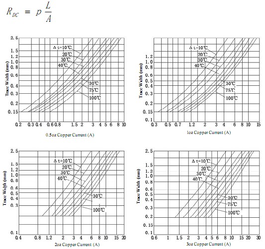
Fig 14 Current Handling Capacity of PCB Trace.
Fig 14 shows the current handling capacity of 0. 5oz-3oz copper with different temp raise.
Printed Circuit Design Tutorial
Section
1. Basic rules in PCB Design : The size and shape of the PCB
2. Basic rules in PCB Design : Define the design rules for the PCB
3. Printed Circuit Design Tutorial (A. V Score)
4. Printed Circuit Design Tutorial (B. Tab-routing)
5. Printed Circuit Design Tutorial (C. Define Non-plated holes - NPTH)
6. Printed Circuit Design Tutorial (D. PCB finishing)
7. Printed Circuit Design Tutorial (E. Solder mask)
8. Printed Circuit Design Tutorial (F. Silk Screen)
9. Printed Circuit Design Tutorial (G. Copper thickness and Via current handling capacity)
10. Printed Circuit Design Tutorial (H. Via)
11. Printed Circuit Design Tutorial (I. Slot)
12. Printed Circuit Design Tutorial (J. Voltage break points)
13. Printed Circuit Design Tutorial (K. Half hole design)
14. PREPARE MANUFACTURE FILES FOR PCB HOUSE
Please login and click here to download the PDF file: Download