

Printed Circuit Design Tutorial (I. Slot)
I. Slot
Slot design can be a headache for a new PCB designer. The major problem for a PCB designer is that you need to make sure the PCB manufacture "KNOW" that there are slots in your design. The easiest way to design a slot is to use multi via overlap with each other to make a slot in the shape you want. In this way the slot will be show up in the NC drill file, as long as you generate the NC drill files right you should be able to see the slot in your design.
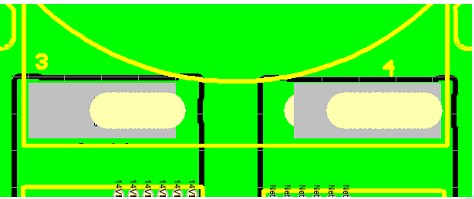
Fig 16 Make slot by using Vias overlap with each other
Fig 16 shows two slots by using vias overlap with each other. With Gold Phoenix the min slot size we can make is 0.65mmX0.7mm.
Printed Circuit Design Tutorial
Section
1. Basic rules in PCB Design : The size and shape of the PCB
2. Basic rules in PCB Design : Define the design rules for the PCB
3. Printed Circuit Design Tutorial (A. V Score)
4. Printed Circuit Design Tutorial (B. Tab-routing)
5. Printed Circuit Design Tutorial (C. Define Non-plated holes - NPTH)
6. Printed Circuit Design Tutorial (D. PCB finishing)
7. Printed Circuit Design Tutorial (E. Solder mask)
8. Printed Circuit Design Tutorial (F. Silk Screen)
9. Printed Circuit Design Tutorial (G. Copper thickness and Via current handling capacity)
10. Printed Circuit Design Tutorial (H. Via)
11. Printed Circuit Design Tutorial (I. Slot)
12. Printed Circuit Design Tutorial (J. Voltage break points)
13. Printed Circuit Design Tutorial (K. Half hole design)
14. PREPARE MANUFACTURE FILES FOR PCB HOUSE
Please login and click here to download the PDF file: Download