

Printed Circuit Design Tutorial (E. Solder mask)
E. Solder mask
Solder mask or solder resist is a lacquer- like layer of polymer that provides a permanent protective coating for the copper traces of a printed circuit board (PCB) and prevents solder from bridging between conductors, thereby preventing short circuits. Solder mask was created primarily to facilitate wave soldering used in mass assembly. Solder mask is traditionally green but is now available in many colors. You can check our website for the different color we can offer, and Gold Phoenix also has the capacity to mix different solder mask color on the same board, if you have this kind requirement you can email us the gerber files and we can send you a quote.
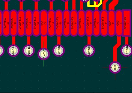
Fig 11 Solder Mask Resolution
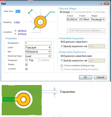
Fig 13 Solder Mask Expansion
When you design the PCB, in the PCB files if the clearance between pads is 4mil that really do not mean that you will have a solder mask dam in the boards you received. Most of the PCB design software has a feature to control the solder mask, called “solder mask expansion”. Due to the limitation of the equipment, the pads on the solder mask layers larger than the pads on the copper, it is impossible have a solder mask opening the same size as the copper pads due to the limitations of the equipment. If we have the mask opening the same size as the copper layer then the solder mask will cover the pads if the mask layer shifts a little during the manufacture process. Most of the PCB house will need solder mask expend 0.1mm=4mil larger than the copper pads, which is shown in Fig 13, in the expansion area there will be no solder mask. For example if on the copper layer the clearance between pads is 12mil, solder mask expansion is 4mil, which means that the clearance on the solder mask layer is 4mil (12mil-4mil*2, 4mil added on two pads), there will be no solder mask between the pads if we use black solder mask, and green solder mask will be hit the most of the manufacture's limit. With Gold Phoenix with green solder mask we need at least 4.5mil clearance between pads, and 6mil clearance for black solder mask in order to print solder mask between pads.
Printed Circuit Design Tutorial
Section
1. Basic rules in PCB Design : The size and shape of the PCB
2. Basic rules in PCB Design : Define the design rules for the PCB
3. Printed Circuit Design Tutorial (A. V Score)
4. Printed Circuit Design Tutorial (B. Tab-routing)
5. Printed Circuit Design Tutorial (C. Define Non-plated holes - NPTH)
6. Printed Circuit Design Tutorial (D. PCB finishing)
7. Printed Circuit Design Tutorial (E. Solder mask)
8. Printed Circuit Design Tutorial (F. Silk Screen)
9. Printed Circuit Design Tutorial (G. Copper thickness and Via current handling capacity)
10. Printed Circuit Design Tutorial (H. Via)
11. Printed Circuit Design Tutorial (I. Slot)
12. Printed Circuit Design Tutorial (J. Voltage break points)
13. Printed Circuit Design Tutorial (K. Half hole design)
14. PREPARE MANUFACTURE FILES FOR PCB HOUSE
Please login and click here to download the PDF file: Download