Printed Circuit Design Tutorial (B. Tab-routing)
B. Tab-routing
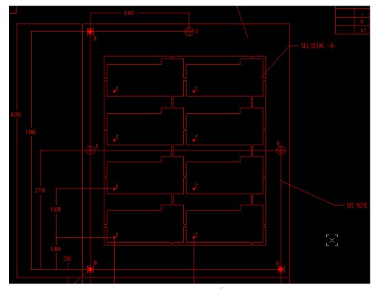
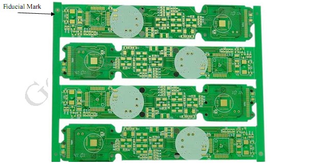
When the board has irregular shape, or the board need a clear edge then the panel need be tab-routed. Fig 8 shows a drawing for the tab -routing panel, Fig 9 is the photo of the tab-routing panel. In the tab-routing panel in order to break the board off the panel after assembly, V score or "mouse bite holes" can be used. Mouse bite holes is a line of holes works the same way as holes on array of stamps . But keep in mind V score will give a clear edge after the boards are break away from the panels, "mouse bite holes" will not give a clear edge.

Fig 8 Tab-routing panel

Fig 9 Photo of a tab-routing panel
Printed Circuit Design Tutorial
Section
1. Basic rules in PCB Design : The size and shape of the PCB
2. Basic rules in PCB Design : Define the design rules for the PCB
3. Printed Circuit Design Tutorial (A. V Score)
4. Printed Circuit Design Tutorial (B. Tab-routing)
5. Printed Circuit Design Tutorial (C. Define Non-plated holes - NPTH)
6. Printed Circuit Design Tutorial (D. PCB finishing)
7. Printed Circuit Design Tutorial (E. Solder mask)
8. Printed Circuit Design Tutorial (F. Silk Screen)
9. Printed Circuit Design Tutorial (G. Copper thickness and Via current handling capacity)
10. Printed Circuit Design Tutorial (H. Via)
11. Printed Circuit Design Tutorial (I. Slot)
12. Printed Circuit Design Tutorial (J. Voltage break points)
13. Printed Circuit Design Tutorial (K. Half hole design)
14. PREPARE MANUFACTURE FILES FOR PCB HOUSE
Please login and click here to download the PDF file: Download


