

Printed Circuit Design Tutorial (H. Via)
H. Via
To estimate via current handling capacity, a via can be equivalent to a trace.
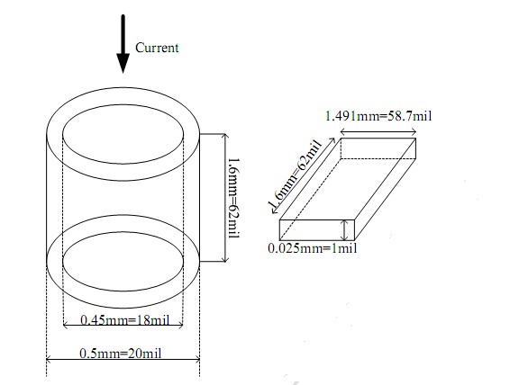
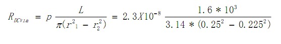
Fig 15 Via in PCB Board equivalent to PCB trace.
Fig 15 shows a via in the PCB. The current will follow through this via from top layer to the bottom layer. There is a 1mil copper plated in the via, this via can be equivalent to a trace with 1.6mm in length, 14.9mm width and 1mil copper thickness. Use the info from section G. the current handling capacity of th is Via can be calculated, 2A is the result. The resistance of the Via can be calculated use following equation, and the result is 0.98mohm at 100 degree, and a 2A current will result a 2mV voltage drop. To increase the current handling capacity a multi via can be place in parallel to reduce the resistance.
Printed Circuit Design Tutorial
Section
1. Basic rules in PCB Design : The size and shape of the PCB
2. Basic rules in PCB Design : Define the design rules for the PCB
3. Printed Circuit Design Tutorial (A. V Score)
4. Printed Circuit Design Tutorial (B. Tab-routing)
5. Printed Circuit Design Tutorial (C. Define Non-plated holes - NPTH)
6. Printed Circuit Design Tutorial (D. PCB finishing)
7. Printed Circuit Design Tutorial (E. Solder mask)
8. Printed Circuit Design Tutorial (F. Silk Screen)
9. Printed Circuit Design Tutorial (G. Copper thickness and Via current handling capacity)
10. Printed Circuit Design Tutorial (H. Via)
11. Printed Circuit Design Tutorial (I. Slot)
12. Printed Circuit Design Tutorial (J. Voltage break points)
13. Printed Circuit Design Tutorial (K. Half hole design)
14. PREPARE MANUFACTURE FILES FOR PCB HOUSE
Please login and click here to download the PDF file: Download