Printed Circuit Design Tutorial (C. Define Non-plated holes- NPTH)
C. Define Non-plated holes(NPTH)
There are several ways to define the non-plated holes in the PCB.
1) You can define certain hole size to be u sed as non-plated holes. For example you can define all 40mil holes in your design to be non-plated, and tell the PCB house you want all 40mil hole to be NPTH
2) You can generate separate NC drill files for NPTH holes.
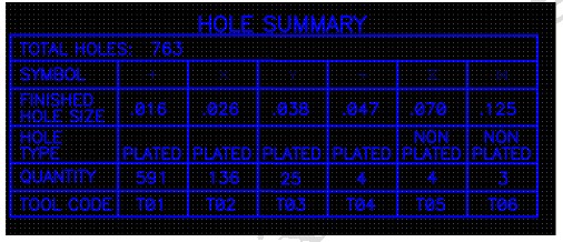
3) The most professional way is to generate a draw chart as shown in Fig 10.

Fig 10 Hole Chart
Printed Circuit Design Tutorial
Section
1. Basic rules in PCB Design : The size and shape of the PCB
2. Basic rules in PCB Design : Define the design rules for the PCB
3. Printed Circuit Design Tutorial (A. V Score)
4. Printed Circuit Design Tutorial (B. Tab-routing)
5. Printed Circuit Design Tutorial (C. Define Non-plated holes - NPTH)
6. Printed Circuit Design Tutorial (D. PCB finishing)
7. Printed Circuit Design Tutorial (E. Solder mask)
8. Printed Circuit Design Tutorial (F. Silk Screen)
9. Printed Circuit Design Tutorial (G. Copper thickness and Via current handling capacity)
10. Printed Circuit Design Tutorial (H. Via)
11. Printed Circuit Design Tutorial (I. Slot)
12. Printed Circuit Design Tutorial (J. Voltage break points)
13. Printed Circuit Design Tutorial (K. Half hole design)
14. PREPARE MANUFACTURE FILES FOR PCB HOUSE
Please login and click here to download the PDF file: Download


