

Printed Circuit Design Tutorial (The size and shape of the PCB)
I.Basic rules in PCB Design
When you first begin to design PCB you need to setup some rules
A.The size and shape of the PCB:
The best way to define the size and shape of the PCB is use mechanical layers as shown in Fig 1. The inner cuts can also be defined on the mechanical layers, just make sure when you generate the Gerber files “SELECT THE mechanical layers”, otherwise your gerber files will not have border.
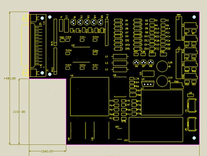
Fig 1Border of the PCB
You can also draw the border on the silk screen layer, but if you have inner cut then you need to be careful. If you draw the inner cuts on the silk layer that will be very confuse for us. Since we will consider it is a “text” symbol. In this case what you can do is shown in Fig 2, put text “CUT OUT”in the silk box.
But define the PCB shape on the mechanical layer is till the “professional way”. The outline tolerance by routing is +/-6mil.
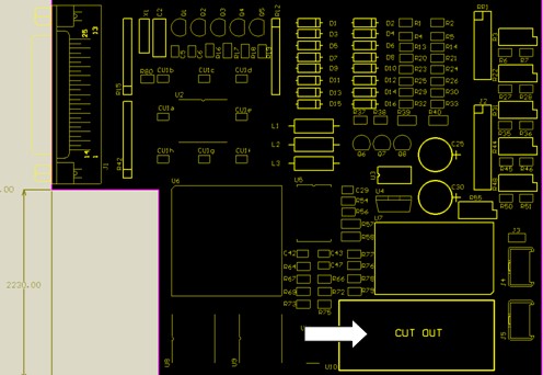
Fig 2 Define cut out in silk layer
Printed Circuit Design Tutorial
Section
1. Basic rules in PCB Design : The size and shape of the PCB
2. Basic rules in PCB Design : Define the design rules for the PCB
3. Printed Circuit Design Tutorial (A. V Score)
4. Printed Circuit Design Tutorial (B. Tab-routing)
5. Printed Circuit Design Tutorial (C. Define Non-plated holes - NPTH)
6. Printed Circuit Design Tutorial (D. PCB finishing)
7. Printed Circuit Design Tutorial (E. Solder mask)
8. Printed Circuit Design Tutorial (F. Silk Screen)
9. Printed Circuit Design Tutorial (G. Copper thickness and Via current handling capacity)
10. Printed Circuit Design Tutorial (H. Via)
11. Printed Circuit Design Tutorial (I. Slot)
12. Printed Circuit Design Tutorial (J. Voltage break points)
13. Printed Circuit Design Tutorial (K. Half hole design)
14. PREPARE MANUFACTURE FILES FOR PCB HOUSE
Please login and click here to download the PDF file: Download