

Printed Circuit Design Tutorial (A. V Score)
II. BASIC TECHNOLOGIES IN PCB MANUFACTURE
In this section we will discuss some basic technologies used in PCB manufacture.
A. V Score
Most of the time we just need individual board , but to increase the efficiency of assembly, or when the board is too small (X,Y dimension less than 1inch ), then we need panelize the small boards to improve manufacturing efficiency.
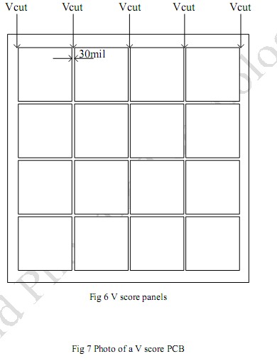
Fig 6 shows a drawing for a V score panel. The clearance between boards is 30mil.Usually we keep the V score clearance 20-40mil. V core can only be used for regular shape board. And the tolerance is +/-6-8mil. In the panel usually we will add a 0.25" blank material around the panel which is called carriers, on the carriers 4 tooling holes and four fiducial marks will be added, this feature is useful for PCB assembly.
Printed Circuit Design Tutorial
Section
1. Basic rules in PCB Design : The size and shape of the PCB
2. Basic rules in PCB Design : Define the design rules for the PCB
3. Printed Circuit Design Tutorial (A. V Score)
4. Printed Circuit Design Tutorial (B. Tab-routing)
5. Printed Circuit Design Tutorial (C. Define Non-plated holes - NPTH)
6. Printed Circuit Design Tutorial (D. PCB finishing)
7. Printed Circuit Design Tutorial (E. Solder mask)
8. Printed Circuit Design Tutorial (F. Silk Screen)
9. Printed Circuit Design Tutorial (G. Copper thickness and Via current handling capacity)
10. Printed Circuit Design Tutorial (H. Via)
11. Printed Circuit Design Tutorial (I. Slot)
12. Printed Circuit Design Tutorial (J. Voltage break points)
13. Printed Circuit Design Tutorial (K. Half hole design)
14. PREPARE MANUFACTURE FILES FOR PCB HOUSE
Please login and click here to download the PDF file: Download